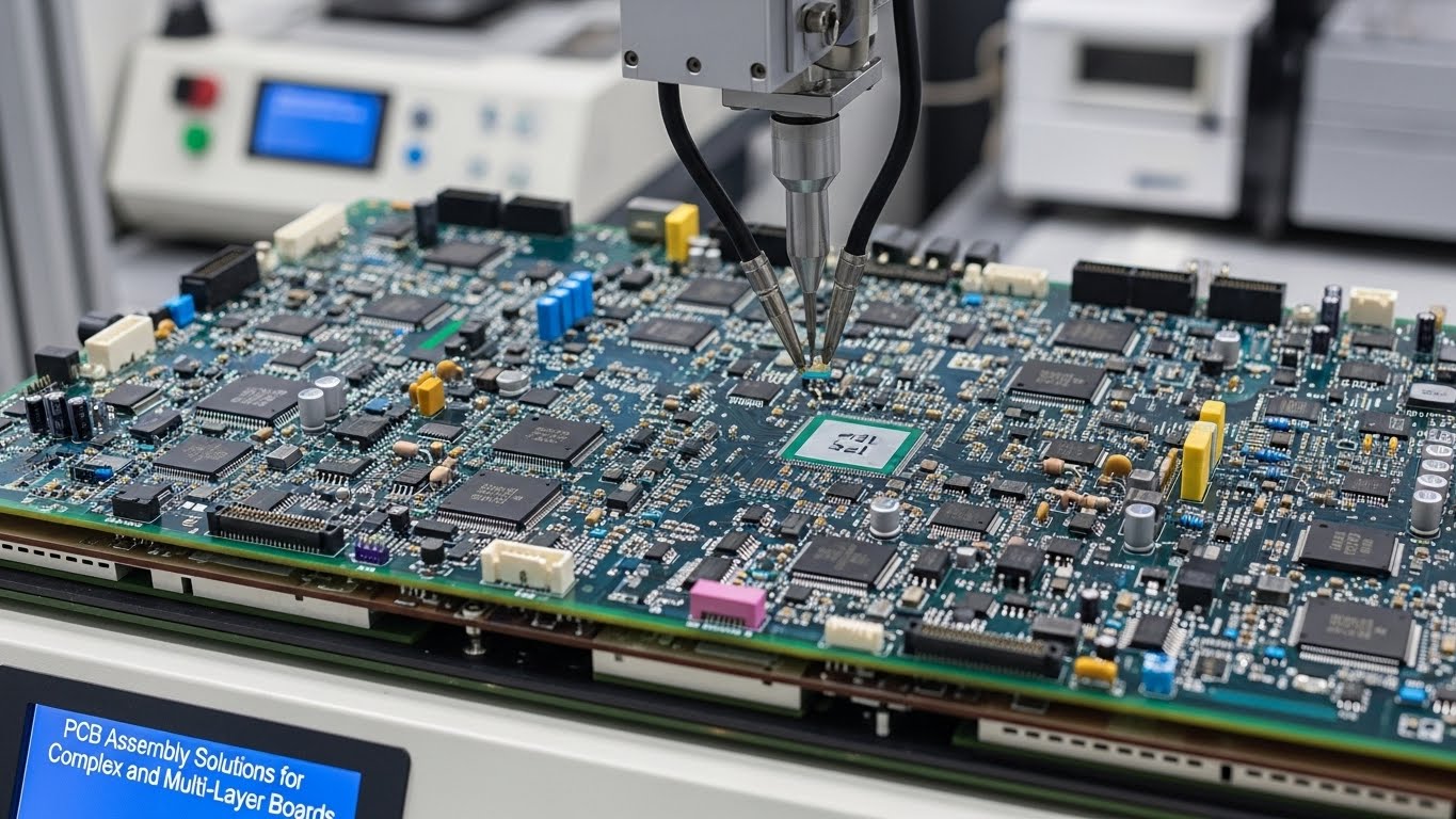
Electronics are shrinking. Devices are getting smarter, faster, and more packed with features than ever before. To make all this happen, the printed circuit boards (PCBs) inside them have had to evolve dramatically. We aren’t just dealing with simple single-layer boards anymore. We are now in the era of high-density, multi-layer marvels.
Assembling these complex boards is no small feat. It requires precision, advanced technology, and a deep understanding of how modern electronics function. Whether you are building medical devices or aerospace controls, you need a partner who understands the intricacies of the process. This is where high-quality custom PCB fabrication and PCBA solutions come into play, bridging the gap between a complex design and a functional reality.
Let’s dive into what makes these boards so challenging and the solutions that make their assembly possible.
The Challenge of Complexity
Why are multi-layer boards so difficult to assemble? It usually comes down to density. You are stacking layers of copper and insulating material, connecting them with tiny vias, and populating them with microscopic components.
Tighter Tolerances
On a standard board, you might have some wiggle room. On a complex multi-layer board, there is zero room for error. Components are placed millimeters apart. If a machine is slightly misaligned, the whole board fails.
Thermal Management Issues
More layers and more power often mean more heat. Complex boards can trap heat inside inner layers. If the assembly process doesn’t account for this, components can overheat and fail during operation.
Signal Integrity
High-speed signals don’t like interference. In a multi-layer stack-up, signals travel vertically through the board. Poor assembly practices can lead to cross-talk or signal loss, turning a smart device into a confused one.
Key Assembly Solutions for Multi-Layer Boards
So, how do manufacturers tackle these challenges? It isn’t just about having better machines. It’s about smarter processes.
1. Advanced Solder Paste Printing
The foundation of a good solder joint is the paste. For fine-pitch components on complex boards, standard stencils won’t cut it.
- Nano-coating stencils: These help the paste release cleanly, ensuring sharp definition for tiny pads.
- 3D Solder Paste Inspection (SPI): Before a single component is placed, machines scan the paste deposits. They check volume, height, and area. If the paste isn’t perfect, the board doesn’t move forward. This prevents defects right at the start.
2. High-Precision Pick and Place
Speed is good, but accuracy is king. Modern pick and place machines use multiple cameras and sensors.
They can handle components as small as 01005 (that’s metric, effectively dust-sized specks). For multi-layer boards, these machines also verify the board’s stretch or shrinkage. PCB materials can shift slightly during manufacturing. High-end placers compensate for this automatically, ensuring the part lands exactly where the pads are, not just where the design file says they should be.
3. Reflow Profiling for Heavy Boards
Multi-layer boards are thick. They have high thermal mass. This means they heat up and cool down slowly.
If you run a thick board through a standard reflow profile, the outer layers might cook while the inner layers stay cool. This leads to “cold solder joints,” which are unreliable connections that break easily.
The solution is a customized thermal profile. Engineers place thermocouples on a test board to measure heat at different points. They tweak the oven zones to ensure the entire board reaches the perfect temperature simultaneously. This guarantees strong, reliable joints from the surface to the core.
4. Automated Optical Inspection (AOI)
You can’t inspect these boards with a magnifying glass. There are simply too many parts.
3D AOI systems are the standard now. They don’t just take a picture; they measure the height of the solder joint. They can spot:
- Lifted leads
- Tombstoning (when a part stands up on one end)
- Insufficient solder
- Coplanarity issues on chips
For complex boards, AOI is the first line of defense against quality escapes.
5. X-Ray Inspection (AXI)
This is crucial for components like BGAs (Ball Grid Arrays). These chips have connections underneath them, hidden from view.
You cannot see these joints with a camera. You need X-rays. X-ray inspection cuts through the layers to reveal the solder balls hidden beneath the chip. It checks for voids (air bubbles) in the solder, bridging (shorts between balls), and alignment. For a 12-layer board with multiple BGAs, X-ray inspection isn’t optional; it’s mandatory.
Design for Assembly (DFA)
The best assembly solution actually starts before the assembly line. It starts with design.
Experienced assembly partners perform a DFA review. They look at your CAD files and spot potential disasters.
- “This part is too close to the edge.”
- “These vias will steal solder from the pad.”
- “You need thermal relief here.”
Catching these issues early saves money. It prevents you from building a batch of expensive, non-functional scrap.
Selecting the Right Partner
Not every assembly house can handle 20-layer boards with blind and buried vias. When you are looking for a partner, ask the hard questions.
- Do they have 3D SPI and AOI?
- What is their smallest component capability?
- Can they handle X-ray inspection in-house?
- Do they offer DFA feedback?
Your partner should be an extension of your engineering team. They should care about the yield as much as you do.
Conclusion
Building complex, multi-layer PCBs is a high-stakes game. The technology demands precision, and the market demands reliability. There are no shortcuts. By leveraging advanced printing, precise placement, and rigorous inspection techniques like X-ray, manufacturers can turn even the most daunting designs into reliable products.
If you are working on the next generation of electronics, don’t leave the assembly to chance. Focus on finding a partner who has the right tools and the right mindset. Quality assembly is the invisible backbone of successful hardware.